The Production Process of Mainstream Integrated Circuits

I. Introduction
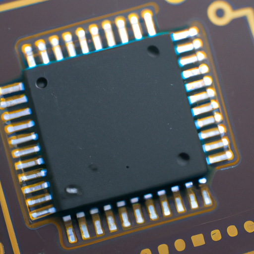
Integrated Circuits (ICs) are the backbone of modern electronics, enabling the functionality of everything from smartphones to supercomputers. These tiny chips, often no larger than a fingernail, contain millions or even billions of transistors that work together to perform complex calculations and tasks. The importance of ICs in contemporary technology cannot be overstated; they are essential for the operation of virtually all electronic devices. This blog post will provide an overview of the intricate production process of mainstream integrated circuits, detailing each phase from design to final testing.
II. Design Phase
The production of integrated circuits begins long before any physical materials are processed. The design phase is crucial, as it lays the groundwork for the entire manufacturing process.
A. Conceptualization and Specification
The first step in the design phase involves gathering requirements and defining functional specifications. Engineers and designers collaborate to understand the intended application of the IC, which influences its architecture and performance criteria. This stage is critical, as any misalignment in specifications can lead to costly redesigns later in the process.
B. Schematic Design
Once the specifications are established, the next step is schematic design. Engineers use Electronic Design Automation (EDA) tools to create circuit diagrams that represent the electrical connections and components of the IC. These tools allow for simulation and verification of the circuit's functionality, ensuring that it meets the specified requirements before moving on to the next stage.
C. Layout Design
The layout design phase involves creating a physical representation of the circuit. This step translates the schematic into a layout that defines the placement of components and the routing of interconnections. Design Rule Checking (DRC) is performed to ensure that the layout adheres to manufacturing constraints, such as minimum spacing between components and layer thicknesses.
III. Fabrication Process
After the design phase is complete, the fabrication process begins. This is where the actual physical ICs are created on silicon wafers.
A. Wafer Preparation
The first step in fabrication is the preparation of silicon wafers. High-purity silicon is melted and crystallized to form cylindrical ingots, which are then sliced into thin wafers. These wafers undergo cleaning and inspection to remove any contaminants and defects, ensuring a pristine surface for subsequent processing.
B. Photolithography
Photolithography is a critical step in the fabrication process. The wafer is coated with a light-sensitive material called photoresist. The wafer is then exposed to ultraviolet (UV) light through a mask that contains the desired circuit pattern. The exposed areas of the photoresist undergo a chemical change, allowing for selective development that reveals the underlying silicon.
C. Etching
Following photolithography, the next step is etching, which removes unwanted material from the wafer. There are two main types of etching: wet etching, which uses chemical solutions, and dry etching, which employs plasma. This process creates the intricate patterns of the circuit by removing the exposed areas of silicon or other materials.
D. Ion Implantation
Ion implantation is used to dope the silicon with impurities, creating n-type and p-type regions essential for transistor operation. By bombarding the silicon with ions of specific elements, manufacturers can control the electrical properties of the material, allowing for the creation of transistors and other components.
E. Deposition
The deposition process involves adding thin films of materials onto the wafer. Two common techniques are Chemical Vapor Deposition (CVD) and Physical Vapor Deposition (PVD). These methods are used to create insulating layers, conductive paths, and other necessary materials that form the complete IC structure.
IV. Assembly Process
Once the fabrication is complete, the ICs undergo an assembly process that prepares them for use in electronic devices.
A. Wafer Testing
Before the wafer is diced into individual chips, it undergoes electrical testing to identify any defective chips. This step is crucial for ensuring that only functional ICs are packaged and sold, reducing waste and improving overall yield.
B. Dicing
Dicing involves cutting the wafer into individual dies, each containing a complete IC. This process requires precision to avoid damaging the delicate structures on the chips. After dicing, careful handling is essential to prevent contamination or physical damage.
C. Packaging
The packaging phase protects the IC and provides a means for connecting it to other components. Various packaging types exist, including Dual In-line Package (DIP), Quad Flat Package (QFP), and Ball Grid Array (BGA). Each type has its advantages and is chosen based on the application and performance requirements.
D. Final Testing
After packaging, the ICs undergo final testing to ensure they function correctly in their intended applications. This includes functional testing, where the IC is evaluated under operational conditions, and quality assurance testing, which assesses reliability and performance over time.
V. Quality Control and Assurance
Quality control is paramount in the production of integrated circuits. The semiconductor industry operates under stringent standards to ensure that ICs meet performance and reliability expectations.
A. Importance of Quality in IC Production
High-quality ICs are essential for the reliability of electronic devices. Defective chips can lead to system failures, safety hazards, and significant financial losses. Therefore, manufacturers invest heavily in quality control measures throughout the production process.
B. Testing Methodologies
Testing methodologies include in-line testing during fabrication, where chips are evaluated at various stages of production, and post-production testing, which assesses the final packaged ICs. These tests help identify defects early and ensure that only high-quality products reach the market.
C. Standards and Certifications
The semiconductor industry adheres to various standards and certifications, such as ISO 9001 and IPC standards, to maintain quality and reliability. Compliance with these standards is crucial for manufacturers to gain customer trust and ensure product safety.
VI. Conclusion
The production process of mainstream integrated circuits is a complex and highly technical endeavor that involves multiple phases, from design to final testing. Each step is critical to ensuring that the final product meets the stringent requirements of modern technology. As the demand for smaller, faster, and more efficient ICs continues to grow, the semiconductor industry is poised for innovation and advancement. Future trends may include the development of new materials, advanced manufacturing techniques, and increased automation, all of which will play a vital role in shaping the future of integrated circuits.
VII. References
1. Academic journals and articles on semiconductor manufacturing.
2. Industry reports and white papers from leading semiconductor companies.
3. Books on IC design and manufacturing processes.
This blog post provides a comprehensive overview of the production process of mainstream integrated circuits, highlighting the intricate steps involved in bringing these essential components to life. As technology continues to evolve, understanding this process becomes increasingly important for anyone interested in the field of electronics.