The Manufacturing Process of Integrated Circuit Layout
I. Introduction
Integrated Circuits (ICs) are the backbone of modern electronics, enabling the functionality of everything from smartphones to supercomputers. These tiny chips, often no larger than a fingernail, contain millions of transistors and other components that work together to perform complex tasks. The manufacturing process of ICs is intricate and highly specialized, involving multiple stages from design to fabrication. This blog post will explore the detailed steps involved in the manufacturing process of integrated circuit layouts, shedding light on the technology that powers our digital world.
II. Understanding Integrated Circuit Layout
A. Definition of IC Layout
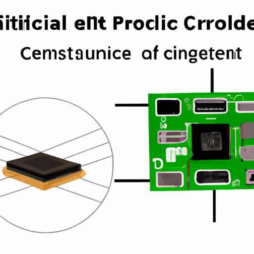
An integrated circuit layout refers to the physical representation of an electronic circuit on a semiconductor chip. It is a blueprint that dictates how various components, such as transistors, capacitors, and interconnects, are arranged and connected on the silicon wafer.
B. Components of an IC Layout
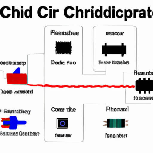
1. **Transistors**: The fundamental building blocks of ICs, transistors act as switches or amplifiers, controlling the flow of electrical signals.
2. **Interconnects**: These are the metal pathways that connect different components within the IC, allowing for communication between transistors and other elements.
3. **Capacitors and Resistors**: These passive components are used for various functions, including filtering, timing, and signal conditioning.
C. Role of Layout in IC Performance
The layout of an IC significantly impacts its performance, including speed, power consumption, and overall functionality. A well-designed layout minimizes signal delays and interference, ensuring that the IC operates efficiently.
III. Design Phase
A. Conceptualization and Specification
The manufacturing process begins with the conceptualization of the IC. Engineers gather requirements and define functional specifications, determining what the IC needs to accomplish.
B. Schematic Design
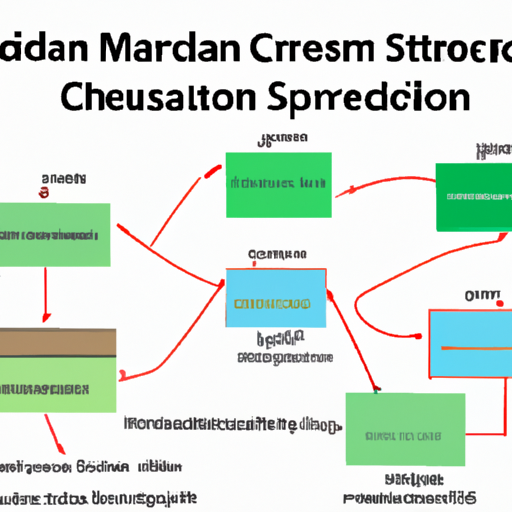
Once the specifications are established, engineers create circuit diagrams, known as schematics. These diagrams represent the electrical connections and components of the circuit. Simulation tools are then used to model the circuit's behavior, allowing designers to identify potential issues before moving to the physical layout.
C. Layout Design
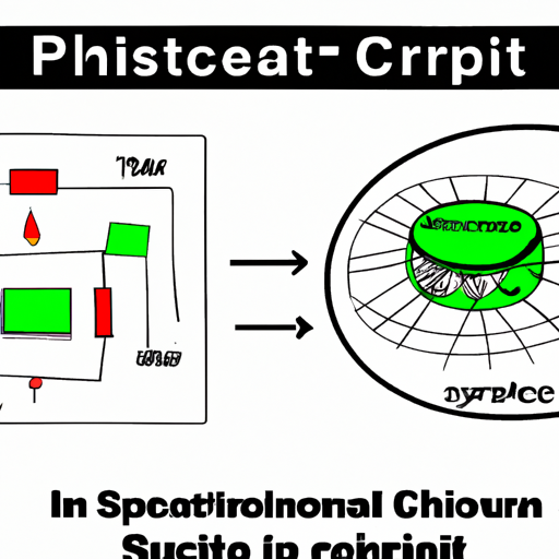
The next step is translating the schematic into a physical layout. This involves using Computer-Aided Design (CAD) software to arrange the components on the silicon wafer. Designers must consider factors such as component size, spacing, and routing of interconnects to optimize performance and manufacturability.
IV. Layout Verification
A. Design Rule Check (DRC)
Before fabrication, the layout undergoes a Design Rule Check (DRC) to ensure compliance with manufacturing rules. These rules dictate the minimum spacing between components, the width of interconnects, and other critical parameters. Common design rules help prevent issues during fabrication that could lead to defects.
B. Layout Versus Schematic (LVS) Check
The next verification step is the Layout Versus Schematic (LVS) check, which compares the physical layout to the original schematic. This process ensures that the layout accurately represents the intended design, confirming that all connections are correct and that the IC will function as intended.
V. Fabrication Process
A. Overview of Semiconductor Fabrication
The fabrication of integrated circuits involves several complex processes that transform a silicon wafer into a functional chip. Each step must be executed with precision to ensure the quality and performance of the final product.
B. Photolithography
Photolithography is a critical step in the fabrication process, where the layout is transferred onto the silicon wafer. A photosensitive material, known as photoresist, is applied to the wafer's surface. The wafer is then exposed to ultraviolet light through a mask that contains the IC layout. The exposed areas of the photoresist are developed, creating a pattern that will guide subsequent processes.
C. Etching
After photolithography, the wafer undergoes etching to remove unwanted material. There are two main types of etching: wet etching, which uses chemical solutions, and dry etching, which employs plasma. This step defines the features of the IC, such as the shapes of transistors and interconnects.
D. Ion Implantation
Ion implantation is used to dope the silicon, creating p-n junctions essential for transistor operation. By introducing impurities into specific areas of the silicon, engineers can control the electrical properties of the material, which is crucial for the performance of the IC.
E. Deposition Techniques
Several deposition techniques are employed to build up layers of materials on the wafer.
1. **Chemical Vapor Deposition (CVD)**: This process involves depositing thin films of materials from gaseous precursors, allowing for precise control over thickness and composition.
2. **Physical Vapor Deposition (PVD)**: In PVD, materials are vaporized and then condensed onto the wafer surface, forming thin films that serve various functions, including insulation and interconnects.
F. Metallization
The final step in the fabrication process is metallization, where metal layers are deposited to create interconnections between components. Common materials used for metallization include aluminum and copper, which provide low-resistance pathways for electrical signals.
VI. Packaging
A. Importance of IC Packaging
Once the IC is fabricated, it must be packaged to protect it from environmental damage and to facilitate its integration into electronic devices. Packaging also provides the necessary connections for the IC to interface with other components.
B. Types of IC Packages
1. **Dual In-line Package (DIP)**: A traditional package with two rows of pins, commonly used for through-hole mounting.
2. **Surface Mount Device (SMD)**: A modern package that allows for mounting directly onto the surface of a circuit board, enabling higher density and smaller designs.
3. **Ball Grid Array (BGA)**: A package with an array of solder balls on the bottom, providing excellent electrical performance and thermal management.
C. Packaging Process
The packaging process involves several steps:
1. **Die Attachment**: The silicon die is attached to the package substrate using adhesives or solder.
2. **Wire Bonding**: Fine wires are used to connect the die to the package leads, establishing electrical connections.
3. **Encapsulation**: The package is sealed with a protective material to safeguard the IC from moisture, dust, and mechanical stress.
VII. Testing and Quality Assurance
A. Importance of Testing in IC Manufacturing
Testing is a critical phase in IC manufacturing, ensuring that the chips meet performance specifications and are free from defects. Rigorous testing helps maintain quality and reliability in the final product.
B. Types of Tests Performed
1. **Functional Testing**: This test verifies that the IC performs its intended functions under various conditions.
2. **Parametric Testing**: Engineers measure electrical parameters, such as voltage and current, to ensure they fall within specified limits.
3. **Reliability Testing**: This involves subjecting the IC to stress conditions, such as temperature and humidity, to assess its long-term performance and durability.
C. Quality Assurance Measures
Quality assurance measures are implemented throughout the manufacturing process, from design to testing. These measures include regular audits, process control, and adherence to industry standards to ensure that the final product meets customer expectations.
VIII. Conclusion
The manufacturing process of integrated circuit layouts is a complex and highly technical endeavor that combines art and science. From the initial design phase to the final testing and packaging, each step is crucial in creating reliable and efficient ICs that power our modern world. As technology continues to evolve, the industry must embrace continuous innovation to meet the growing demands for smaller, faster, and more powerful integrated circuits.
IX. References
For those interested in further exploring the intricacies of IC manufacturing processes, the following resources are recommended:
1. "Microelectronics: Circuit Analysis and Design" by David A. Neamen
2. "Semiconductor Manufacturing Technology" by David A. Hodges and Horace G. Jackson
3. Online courses and tutorials on semiconductor fabrication and IC design from platforms like Coursera and edX.
By understanding the manufacturing process of integrated circuits, we can appreciate the remarkable technology that drives our digital age and the engineers who make it all possible.

